1. Introduction
The Common Collector (CC) circuit is a type of bipolar junction transistor (BJT) configuration, where the input signal is applied to the Base terminal and the output signal is taken from the Emitter terminal. Thus the Collector terminal is common to both the input and output circuits. This type of configuration is called Common Collector, (CC) because the collector terminal is effectively “grounded” or “earthed” through the power supply.
The Emitter Follower is a buffer stage with high input impedance, low output impedance, and a gain of approximately unity. Using the small-signal low-frequency circuit, we will find the gain, input resistance seen at the base, and output resistance seen at the emitter. The Hybrid model is a popular circuit model used for analyzing the small signal behavior of bipolar junction and field effect transistors.
As we traverse through the Small Signal Analysis for the Emitter Follower (CC) circuit, we gain knowledge about the Hybrid model (BJT parameters) and study the calculation of Voltage Gain, Input Impedance, Output Impedance and Current Source Biasing in detail.
2. Small Signal Analysis
Small signal analysis is a common modeling technique that is used to approximate the behavior of electronic circuits containing nonlinear devices with linear equations.
Small-signal analysis consists of:
- Finding the quiescent or operating point of a circuit. This is found by zeroing all signal sources leaving just the DC sources and then solving for the DC voltages and currents in the circuit.
- Linearizing the nonlinear circuit elements at the operating point. For example, a diode is replaced with a resistor that models the dynamic resistance at the particular operating point. The dynamic, or small-signal resistance is the ratio of the change in voltage to a small (actually infinitesimal) change in current from the operating point.
- Finding the small-signal solution. The DC sources are zeroed, the signal sources are activated, and linear circuit analysis is used to solve for the small-signal voltages and currents.
Having solved for the small-signal voltages and currents, the total solution is simply the sum of the DC solution and the small-signal solution. This total solution is an approximation that is valid only when the signals are in some sense small, i.e., that the variations of the voltages and currents in the circuit are small relative to the DC voltages and currents. [1]
Small Signal Performance Parameters:
In AC analysis, we are interested to find
- Voltage Gain
- Input Resistance or impedance
- Output Resistance or impedance
The hybrid model and hybrid T models are the two popular models for small signal analysis.
3. Hybrid Model
3.1. Introduction
The hybrid model is a popular circuit model used for analyzing the small signal behavior of bipolar junction and field effect transistors. Sometimes it is also called the Giacoletto model because it was introduced by L.J. Giacoletto in 1969. The model can be quite accurate for low-frequency circuits and can easily be adapted for higher frequency circuits with the addition of appropriate interelectrode capacitances and other parasitic elements.
3.2. BJT Parameters
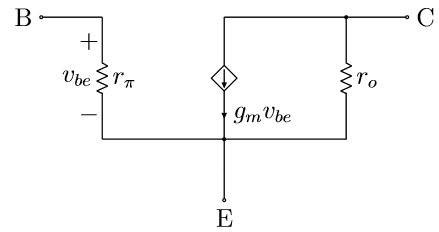
The hybrid model is a linearized two-port network approximation to the BJT using the small-signal base-emitter voltage, , and collector-emitter voltage, , as independent variables, and the small-signal base current, , and collector current, , as dependent variables.
A basic, low-frequency hybrid model for the bipolar transistor is shown in figure 1. The various parameters are as follows.
(evaluated at ) =
is the transconductance, evaluated in a simple model, where:
- = quiescent collector current (collector bias or DC collector current)
-
, where,
= Boltzmann’s constant = ,
= the charge of an electron = ,
= the transistor temperature in kelvinAt approximately room temperature (295 K, 22 °C), is about .
-
(evaluated at ) = = where,
= DC (bias) base current,
= current gain at low frequency
= (evaluated at ) =The output conductance, gce, is the reciprocal of the output resistance, r0:
.The transresistance, rm, is the reciprocal of the transconductance:
.[2]
4. Small Signal Analysis for Emitter Follower
4.1. Hybrid Model of Emitter Follower
Common collector (CC) configuration is a very important circuit which finds frequent applications in the design of both small-signal and large-signal amplifiers and also in digital circuits. The circuit is also known as an emitter follower, the reason for which is explained below.
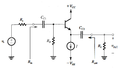
The circuit of the CC configuration is shown below in figure 2. Since the collector is to be at signal ground, the collector resistance is removed. The input signal is capacitively coupled to the base, the output signal is capacitively coupled from the emitter to a load resistance . [3]
Bias current will determine , , and .
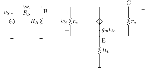
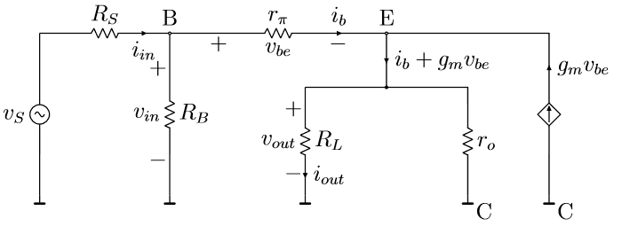
Drawing the circuit in its hybrid equivalent:
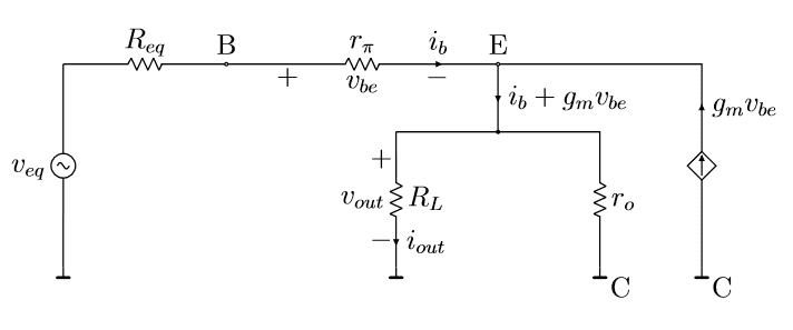
Simplifying the above circuit shown in figure 3:
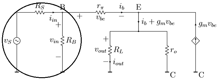
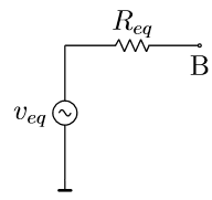
The Thevenin equivalent circuit of the encircled portion:
Clearly, the equivalent voltage and resistance are:
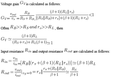
4.2. Calculation of Voltage Gain
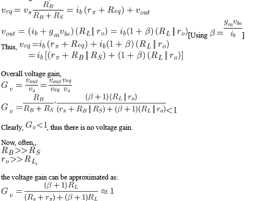
Using and in figure 4:
Now using KVL,
Now as is close to unity, the voltage at the emitter () follows very closely the voltage at the input, which gives the circuit the name emitter follower. [4]
4.3. Calculation of Input Impedance
Here can be taken as ∞ and considering , input impedance can be approximated to:
Since, 𝛽 is typically of the order of 100, the input impedance is ~100 times greater than . For , .
Comparing this with the input resistance of the common-emitter circuit, we see that the emitter follower has much higher input resistance. [4]
4.4. Calculation of Output Impedance
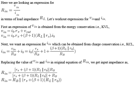
Here we are looking for an expression for:
Let’s work out expressions for and .
First an expression of is obtained from the energy conservation, i.e., KVL:
Next, we want an expression for which can be obtained from charge conservation, i.e., KCL:
Replacing the value of and in original equation of Rout, we get output impedance as,
If , , and , then:
Thus, the output resistance of the emitter follower is low, a result of its impedance transformation or buffering action, which leads to the division of by . [3]
4.5. Biased By Current Source
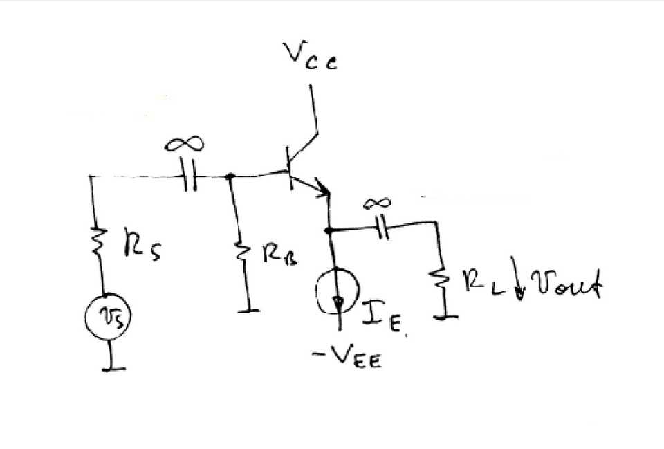
In the above figure, an Input is provided at the Base, Output is obtained from Emitter and there is no need for a bypass capacitor.
A current source () is added at the output of an emitter follower topology at the emitter leg of the transistor. The reason for this is as follows:
When biasing a transistor, we want the Q point to be stable. Since varies a lot, we want to design in such a way that changes in do not disturb the bias point.
By placing a current source there, will not depend on (and ) and that way we can keep the transistor in the active region regardless of changes in . [5]
4.6. Summary
Here we start with biased DC analysis. We make sure that BJT is in FA (Forward Active) mode, and then we calculate small signal parameters for AC analysis.
An emitter follower can be used as a voltage buffer circuit as it delivers voltage from source to load. [4]
5. Conclusion
To conclude, the emitter follower exhibits a high input resistance, a low output resistance, a voltage gain that is smaller than but close to unity, and a relatively large current gain. It is therefore ideally suited for applications in which a high-resistance source is to be connected to a low-resistance load — namely, as the last stage or output stage in a multistage amplifier, where its purpose would be not to supply additional voltage gain but rather to give the cascade amplifier a low output resistance. [3]
6. References
[1] Alfred Centauri, “What does small signal analysis mean?”, URL: https://electronics.stackexchange.com/a/91620, (Accessed: June 9, 2020).
[2] Wikipedia, “Hybrid-pi model”, URL: https://en.wikipedia.org/wiki/Hybrid-pi_model, (Accessed: June 9, 2020)
[3] Adel S. Sedra, Kenneth C. Smith, “Microelectronic Circuits”, 6th Edition. Oxford University Press 2004, Chap. 5: Bipolar Junction Transistors (BJTs).
[4] Leon Shterengas, “ESE372/Lecture19”, URL: http://www.ece.sunysb.edu/~oe/Leon/ESE372/Lecture19.pdf, (Accessed: June 7, 2020)
[5] Big6, “The need for a current source in an emitter follower”, URL: https://electronics.stackexchange.com/a/281486, (Accessed: June 11, 2020)
